Define The Term Forbidden Energy Gap
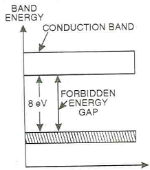
Width of the forbidden energy gap depends upon the nature of the substance. The forbidden gap energy is of the order of 07eV for Ge and 11eV for Si.
Difference Between Conductor Semiconductor And Insulator With Comparison Chart Electronics Desk
The superconducting energy gap is a key aspect in the theoretical description of superconductivity and thus features prominently in BCS theory.
Define the term forbidden energy gap. In solid-state physics the energy gap or the band gap is an energy range between valence band and conduction band where electron states are forbidden. In contrast to conductors electrons in a semiconductor must obtain energy eg. With a small amount of energy that is supplied the electrons can easily jump from the valence band to the conduction band.
Forbidden energy gap Eg. The portion of the energy band structure of a semiconductor or insulator between the valence and conduction bands. There are no electrons in the conduction band.
The electrons in valence band cannot move because they are locked up between the atoms. In other words the energy required by an electron to jump from valence band. Forbidden energy gap is the gap between valence band and conduction band.
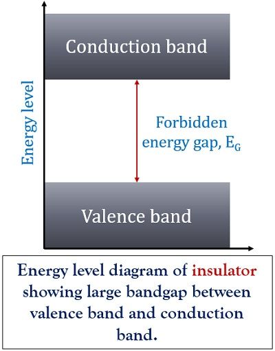
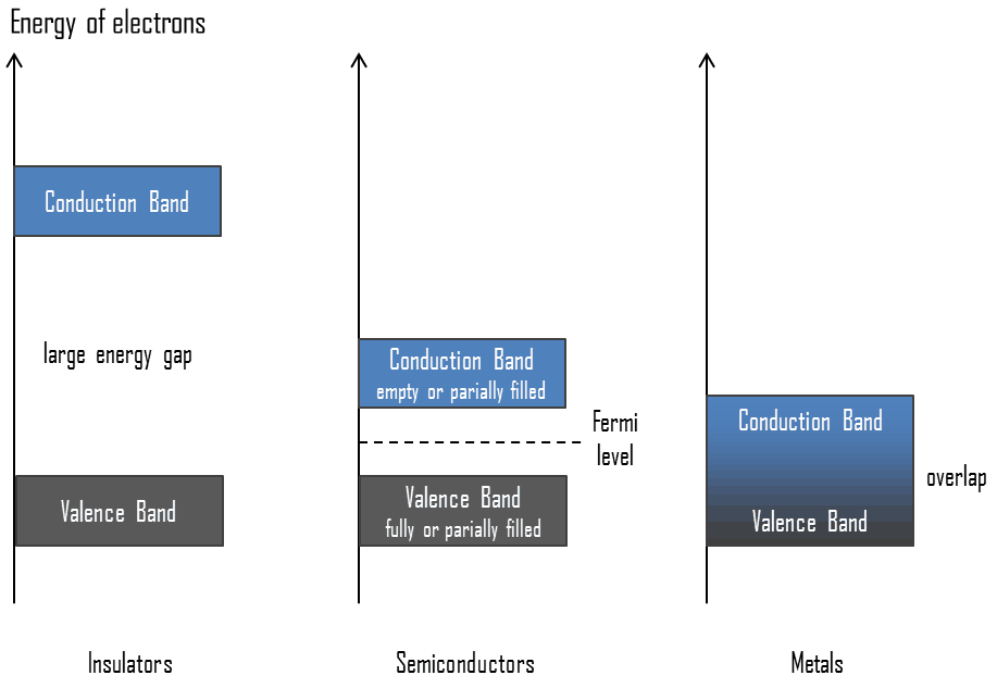
From ionizing radiation to cross the band gap and to reach the conduction band. The energy required to transfer an electron from valence band to conduction band the external energy which is required is equal to the forbidden energy gap. The forbidden gap between the valence band and conduction band is very large in insulators.
Electrons are not found in this band. For superconductors the energy gap is a region of suppressed density of states around the Fermi energy with the size of the energy gap much smaller than the energy scale of the band structure. FEB is completely empty.
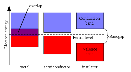
Forbidden energy gap. Answer Forbidden zone is the energy gap between valence band and conduction band in solids this gap is large in insulators and small in semi conductors. Electrons are able to jump from one band to another.
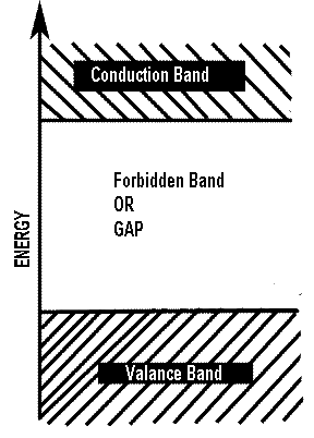
Separating these two bands is an energy gap termed the forbidden gap in which electrons cannot normally exist. Two such states are found in the first forbidden energy gap and because of their localization properties called the Tamm-like and adsorptionlike states. The energy gap of insulator is approximately equal to 15 electron volts eV.
It is the electronic energy band where there is no electron state exists due to quantization energy. So thats all from this article. What is a Forbidden Energy Gap.
No free electron is present in the forbidden energy gap. The valence band is completely filled at 0 K. The minimum energy required for shifting electrons from the valence band to the conduction band is called band gap leftE_gright.
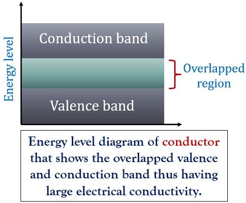
There is no forbidden zone in metals because in metals valence and conduction band overlap. What is the order of forbidden gap in the energy bands of silicon. The band obtained by separating conduction band and valence band is called as forbidden energy band or forbidden gap.
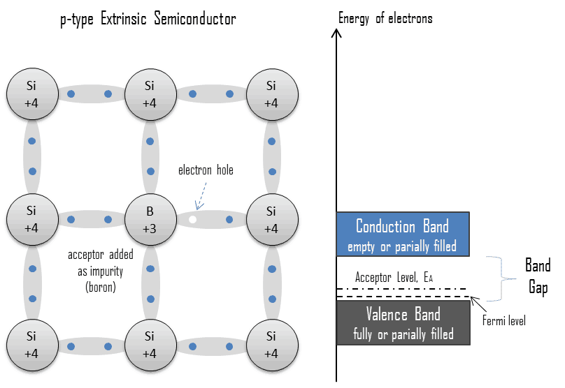
Forbidden energy gap is also known as Fermi energy level. Forbidden energy gap E g is the difference of energy levels of conduction band and within conduction band. This portion does not contain a continuum of states as do the valence and conduction bands but may contain discrete states introduced by dopant or deep level impurities in the material.
What is meant by the term forbidden zone in reference to band theory of solids. The data are explained in the light of extrensic and lattice vibrations and the width of the forbidden energy gap properties. Forbidden energy gap or energy gap or band gap or band or Eg is the gap between the top of the valance band and bottom of the conduction band.
In semiconductors and insulators electrons are confined to a number of bands of energy and forbidden from other regions. The forbidden gap in the energy bands of silicon is a 26 eV b 11 eV c 01 eV d 6 eV asked Jan 17 2019 in Physics by Maryam 792k points semiconductor electronics. I hope you get the idea about the Classification of the solids according to the Forbidden energy gaps.
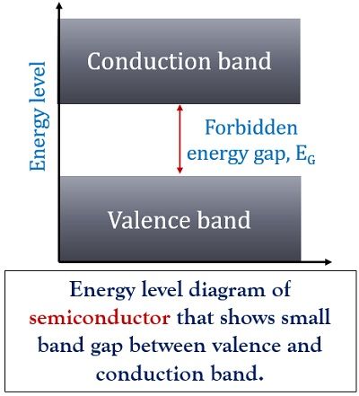
- Here we give solutions for every questions you ask us. The term band gap refers to the energy difference between the top of the valence band and the bottom of the conduction band. Energy gap between the conduction band and valence band is known as the forbidden energy gap ie E g CB min - VB max.
The energy gap between the valence band and conduction band is called the forbidden energy gap.
Why The Conduction Band Is Empty Quora

Chapter 2 Energy Bands And Effective Mass Ppt Video Online Download

How Is Drift Current Produced In Semiconductors Quora
Why The Conduction Band Is Empty Quora

The Forbidden Energy Band Gap In Conductors Semiconductors And Insulators Are Eg 1 Eg 2 And Eg 3 Respectively The Relation Among Them Is

Chapter 2 Energy Bands And Effective Mass Ppt Video Online Download
Difference Between Conductor Semiconductor And Insulator With Comparison Chart Electronics Desk

Chapter 2 Energy Bands And Effective Mass Ppt Video Online Download

Difference Between Valance Band Conduction Band And Energy Band Youtube
What Is Semiconductivity Band Theory Definition
Explain How Conduction Takes Place In Insulators Electrical Engineering
Why The Conduction Band Is Empty Quora
What Is Semiconductivity Band Theory Definition
Difference Between Conductor Semiconductor And Insulator With Comparison Chart Electronics Desk

The Forbidden Energy Band Gap In Conductors Semiconductors And Insulators Are Eg 1 Eg 2 And Eg 3 Respectively The Relation Among Them Is
Energy Bands Insulator Conductor Semiconductor D E Notes
Valence Band Energy Education

Band Theory Of Solids Definition Valence Band Conduction Band

Chapter 2 Energy Bands And Effective Mass Ppt Video Online Download
Post a Comment for "Define The Term Forbidden Energy Gap"